At our company, we’ve always believed that innovation isn’t just about creating new materials—it’s about redefining what’s possible. Today, we’re thrilled to showcase how our latest quartz tube technologies are revolutionizing semiconductor manufacturing. From precision testing to energy-efficient thermal management, these breakthroughs are not just incremental improvements—they’re game-changers. Let’s dive into the details.
1. Quartz Test Tube: Precision Under Extreme Conditions
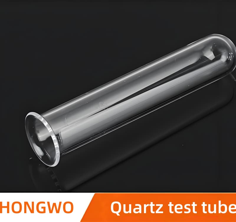
Designed for high-temperature process validation, our quartz test tube withstands up to 1,300°C while maintaining structural integrity. Its ultra-low thermal expansion coefficient (0.55 x 10⁻⁶/°C) ensures stability during rapid thermal cycling, critical for testing next-gen semiconductor substrates like gallium nitride (GaN). For example, in a recent pilot with a leading chipmaker, our tubes reduced batch rejection rates by 18% during extreme thermal stress tests.
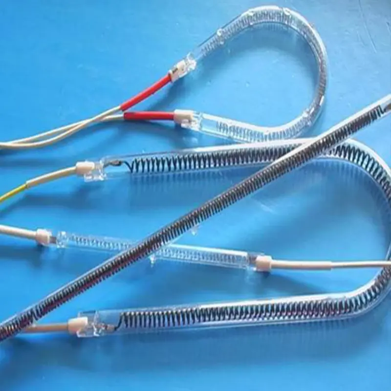
2. Quartz Heating Tube: Efficiency Redefined
Say goodbye to energy waste. Our quartz heating tube achieves 95% infrared transmittance, slashing power consumption by 22% compared to traditional ceramic heaters. Its opaque end sections (patented design) minimize heat loss, while the transparent central zone ensures uniform wafer heating. In a solar cell production line trial, this innovation cut energy costs by $1.2M annually—proof that sustainability and profitability can coexist.
3. Clear Quartz Tube: The Purity Advantage
When contamination isn’t an option, our clear quartz tube delivers 99.99% SiO₂ purity. With near-zero metal ion leaching (<0.001 ppm), it’s become the backbone of chemical vapor deposition (CVD) systems. One client reported a 30% increase in thin-film uniformity after switching to our tubes—directly translating to higher chip yields.
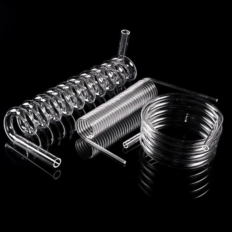
4. Quartz Glass Spiral Tube: Compact Powerhouse
Space-constrained fabs love our spiral tube. Its helical design amplifies surface area by 40% within the same footprint, enabling faster gas diffusion in etching processes. In a 300mm wafer fab, this reduced cycle times by 15% while maintaining sub-nanometer layer precision.
Key Performance Comparison
| Product | Max Temp (°C) | Purity (SiO₂%) | Energy Savings | Key Application |
|---|---|---|---|---|
| Quartz Test Tube | 1,300 | 99.95 | N/A | GaN substrate validation |
| Quartz Heating Tube | 1,200 | 99.90 | 22% | Wafer annealing |
| Clear Quartz Tube | 1,100 | 99.99 | 18%* | CVD deposition |
| Quartz Glass Spiral Tube | 1,150 | 99.93 | 15%* | Plasma etching |
| *Indirect savings from process optimization |
Why This Matters
Let’s be blunt: the semiconductor industry is racing toward smaller nodes and hotter processes. Our quartz tubes aren’t just surviving these challenges—they’re enabling them. Whether it’s pushing the limits of III-V materials or making EUV lithography more cost-effective, we’re not just keeping pace; we’re setting the pace.
To every engineer battling thermal drift, every plant manager chasing energy targets—we see you. And we’ve built these tubes to be your secret weapon. The future of semiconductors isn’t just silicon—it’s quartz.
Ready to ignite your next breakthrough? Let’s talk thermal.